MicroTec for Two-Dimensional Semiconductor Process and Device Simulation: Development Status Update

Waterloo, Ontario, Canada (PRWEB) September 27, 2017 -- Siborg Systems Inc. from Waterloo, Ontario, has been working with Sensor Creations Inc. in Camarillo, California, for the past two years in developing a practical tool for simulating process flow and optical sensor performance.
Sensor Creations Inc. and Siborg Systems Inc. came together to develop both semiconductor device and process simulation for optical sensor structures. The optical sensors, due to their large sizes, require many steps during fabrication such as implantation, depositions, epitaxial growth, annealing and oxidation, etching, etc. When simulating these optical sensors, the size contributes to high CPU time when using conventional simulation tools. MicroTec, on the other hand, was able to run a typical process simulation on a regular PC within a few minutes.
MicroTec is useful for steady-state two-dimensional semiconductor device simulation but is insufficient for capacitance extraction. A new method to calculate capacitance of a semiconductor structure by solving equations for the total current conservation was created. This method is applicable for 1D, 2D and 3D structures, but is limited to low-leakage conditions and low frequencies. The most straightforward method for solving the equation of total current conservation, mutual capacitances may be calculated using the formula C=Idt/dV.
The formula can be improved by using a relation that involves both resistances and capacitances. In order to include both, one more data point is required. Including both resistances and capacitances may make the formula more accurate but it is still not equivalent to the actual compact model of the semiconductor structure because it is a set of interconnected transmission lines and therefore any simplification of the equivalent circuit results in less accuracy. The current method is inaccurate and requires simulation with a properly selected ramp speed. If the speed is too slow, the displacement current becomes too small and is swamped by the numerical noise; if the speed is too fast, the voltage drop due to Ohm’s law distorts the capacitance. The high sensitivity to the ramp time makes this application limited in use.
Unlike the current method, the charge method uses charges affiliated with the contacts rather than the currents. This eliminates the issue of result interpretation using equivalent R-C circuit. The same equation is used in both charge and current methods, but instead of calculating currents, we use the response to the excitation applied to a contact as a weight function when integrating the charge in the structure. Using a convolution of the “affiliation” function with carrier density, the charges are calculated. This charge method seemed stable and accurate and was used successfully for the calculation of capacitance in optical sensors.
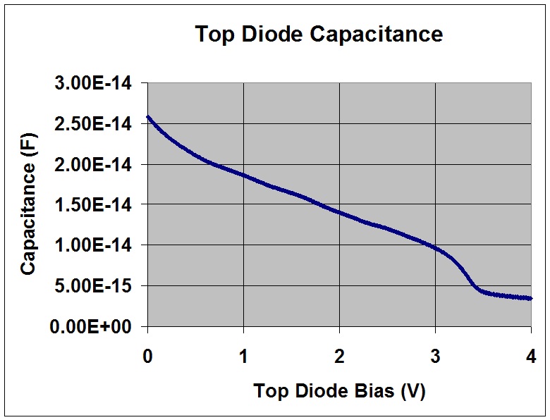
The included picture shows the capacitance calculated by the charge based method at various ramp speeds.
All 4 curves virtually coincide when the capacitance is calculated using the charge based method at various ramp speeds, as depicted in the included picture. This charge based method’s application is questionable when significant minority charge is interjected, i.e. with forward biased junctions. The charged based method requires more research, but has shown to have more applications.
“We have been using two-dimensional semiconductor process and device simulation software MicroTec from Siborg intensively for the last couple of years. We found it very useful in our practical optical sensor prototype development. It significantly outperforms other available commercial tools by the speed, robustness and how easy it is to use. Last, but not least, the license cost is significantly lower as well.” Says Sensor Creations’ Stefan Lauxtermann.
MicroTec is a TCAD tool that has been primarily used by smaller semiconductor companies but also by major semiconductor manufacturers such as Integrated Device Technology, Hitachi, National Semiconductor, Matasushita, etc. Most of our clients are in power semiconductors and solar cell industry.
As an educational semiconductor process and device simulation tool, MicroTec and three-dimensional heat transfer equation solver SibLin are simple and easy to learn.
Michael Obrecht, Siborg Systems Inc., http://www.smarttweezers.us, +1 (519) 888-9906, [email protected]
Share this article